Page 1 of 6
MCP3561/2/4 MCP3564 Click Board
Posted: Sun Jul 11, 2021 1:32 pm
by SpeedPIC32
General DescriptionThe MCP3561/2/4 devices are 2/4/8-channel, 24-bit,Delta-Sigma Analog-to-Digital Converters (ADCs) withprogrammable data rate of up to 153.6 ksps. They offerintegrated features, such as internal oscillator, tem-perature sensor and burnout sensor detection, in orderto reduce system component count and total solutioncost.The MCP3561/2/4 ADCs are fully configurable withOversampling Ratio (OSR), from 32 to 98304, and gainfrom 1/3x to 64x. These devices include an internalsequencer (SCAN mode) with multiple monitorchannels and a 24-bit timer to be able to automaticallycreate conversion loop sequences without needingMCU communications. Advanced security features,such as CRC and register map lock, can ensure config-uration locking and integrity, as well as communicationdata integrity for secure environments.These devices come with a 20 MHz SPI-compatibleserial interface. Communication is largely simplifiedwith 8-bit commands, including various ContinuousRead/Write modes and 24/32-bit multiple data formatsthat can be accessed by the Direct Memory Access(DMA) of an 8-bit, 16-bit or 32-bit MCU.
MCP3564 Click Board
Part Number: MIKROE-4105
ummary:
ADC 9 Click is 8th channel analog to digital converter expansion board, for projects where you have demand for multi channel ADC conversion such as microcontrollers with small number or none analog inputs. This Click board is based on MCP3564 a 24-bit Delta-Sigma Analog-to-Digital Converter with programmable data rate of up to 153.6 ksps from Microchip. It offers integrated features, such as
http://https//www.mikroe.com/adc-9-click
hello
would like to see the chip(s) under sensors.
Would like to build a pid controller with it
greetings speedpic32
Re: MCP3561/2/4 MCP3564 Click Board
Posted: Tue Jul 13, 2021 4:22 pm
by BenR
Hello,
Thanks for the suggestion I will see if I can get my hands on one and give it a go for you.
Re: MCP3561/2/4 MCP3564 Click Board
Posted: Thu Jul 22, 2021 8:13 pm
by SpeedPIC32
Hello,
can you already estimate when the chip will be processed?
I can also send a clickboard if it is faster then?
With kind regards
Re: MCP3561/2/4 MCP3564 Click Board
Posted: Fri Jul 23, 2021 12:29 pm
by BenR
Hello,
If you have one available you could send us then that would certainly help with testing and with debugging any problems you encounter. Maybe see how you get on first.
I've now created a component for you and tried to keep it as simple as possible with just an initialise and sample macros. It may be too simple and you may want some of the more advanced features of the device, if this is the case then let us know the specifics of what you need. I can also share the component source project if you want to be more in control of what's available.
The sample macro allows you to to specify the positive channel and negative channel so you can use the ADC in differential mode or you can lock one of the channels to VDD/GND for independent inputs.
Let us know how you're getting on.
Re: MCP3561/2/4 MCP3564 Click Board
Posted: Mon Jul 26, 2021 4:00 pm
by SpeedPIC32
hello
if i set the positive and negative channels to analogue ground, or both to the same ground, the output value should actually be around 0, i think.
the same if i set the selection to 0 and 1 and short circuit the inputs.
is always
16777215<CR><LF>
16776959<CR><LF>
16776703<CR><LF>
16776959<CR><LF>
16776959<CR><LF>
16776703<CR><LF>
16776703<CR><LF>
16777215<CR><LF>
8 and 12 results in
<CR><LF>
16777215<CR><LF>
255<CR><LF>
255<CR><LF>
511<CR><LF>
511<CR><LF>
16777215<CR><LF>
255<CR><LF>
255<CR><LF>
255<CR><LF>
511<CR><LF>
511<CR><LF>
511<CR><LF>
511<CR><LF>
511<CR><LF>
255<CR><LF>
511<CR><LF>
511<CR><LF>
255<CR><LF>
511<CR><LF>
255<CR><LF>
255<CR><LF>
255<CR><LF>
511<CR><LF>
255<CR><LF>
16777215<CR><LF>
please check once
with best regards
Re: MCP3561/2/4 MCP3564 Click Board
Posted: Tue Jul 27, 2021 11:31 am
by BenR
Hello,
In your program you are sampling between 8 and 12 which equates to GND and REF-. Hopefully this is all that is wrong.
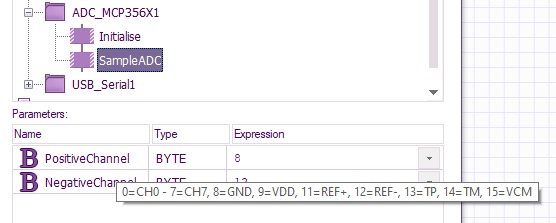
- Tooltip.jpg (24.06 KiB) Viewed 14046 times
I'm not sure what is suppost to happen here. It could be you are suppost to get 0 but I can't say for sure. What happens if you select a valid ADC input channel for the positive and GND or VREF- as the negative?
Re: MCP3561/2/4 MCP3564 Click Board
Posted: Wed Jul 28, 2021 12:37 am
by SpeedPIC32
Hello
the positive reference is 2048 millivolts.
if i switch the positive channel to 11 and the negative to 8 or 12 the ADC should output a value of +8388608. that is 2^23. as the ADC has no negative reference. REF- is equal to GND or 0.
The ADC always converts the difference of the two inputs.
The board can only output +8388608 or -8388608 at gain 1 because there is no -Ref voltage of 2048 millivolts.
If the difference of the input voltage is 0, 0 must also be output. This means that without voltage at the inputs the output value is 0 and this should be the case if both channels are equal, e.g. both at 8 or both at 0 or at 0 and 1 without voltage with a short circuit.
Excerpt from the data sheet
Differential Reference Voltage
Inputs: REFIN+, REFINThe REFIN+ pin is the noninverting differential
reference input (VREF+).
The REFIN- pin is the inverting differential reference
input (VREF-).
For single-ended reference applications, the REFINpin should be directly connected to AGND.
The differential reference voltage pins must respect
this condition at all times: 0.6V ≤ VREF ≤ AVDD. The
differential reference voltage input is given by the
following equation:
VREF = VREF+ – VREF
Analog Inputs (CHn): Differential
or Single-Ended
The CHn pins are the analog input signal pins for the
ADC. Two analog multiplexers are used to connect the
CHn pins to the VIN+/VIN- analog inputs of the ADC.
Each multiplexer independently selects one input to be
connected to an ADC input (VIN+ or VIN-). Each CHn
pin can either be connected to the VIN+ or VIN- inputs
of the ADC. This multiplexer selection is controlled by
either the MUX register in MUX mode or the SCAN
register in SCAN mode. See Figure 5-1 for more details
on the multiplexer structure.
When the input is selected by the multiplexer, the differential (VIN) and Common-Mode Voltage (VINCOM) at
the ADC inputs are defined by:
VIN = VIN+ – VIN-
with best regards SpeedPic32
Re: MCP3561/2/4 MCP3564 Click Board
Posted: Wed Jul 28, 2021 12:48 am
by SpeedPIC32
What I did in the previous post is a test to see if everything is in order.
REF+ must bring +8388608 and 0 = 0 and -2048millivolt -8388608
Re: MCP3561/2/4 MCP3564 Click Board
Posted: Thu Jul 29, 2021 7:44 pm
by BenR
Thanks, I'll have another dig through the component code and compare to an existing library to see if I can spot any problems.
Re: MCP3561/2/4 MCP3564 Click Board
Posted: Thu Jul 29, 2021 9:51 pm
by SpeedPIC32
Hello and thank you.
Question: how does the chip work?
Does it convert constantly?
If so, at what data rate?
can the scanner mode still be integrated?
How does the IRQ mode work at the moment?
With kind regards