Component: CAN (Internal, MCP2515) (Comms: Interface)

From Flowcode Help
Revision as of 16:17, 7 January 2022 by Wiki bot (talk | contribs)
Jump to navigationJump to search
Author Matrix Ltd
Version 2.10
Category Comms: Interface


CAN (Internal, MCP2515) component

Low level routines for controling the CAN interface either using an external MCP2515 IC and a SPI bus connection or using an internal CAN peripheral if available on your device. Both methods will require a CAN driver IC like the MCP2551 to drive the CAN signals on the bus.

Component Pack

COMMSA

Detailed description

No detailed description exists yet for this component

Examples

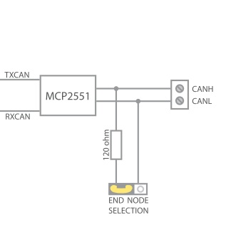
Internal CAN schematic

InternalCAN.jpg


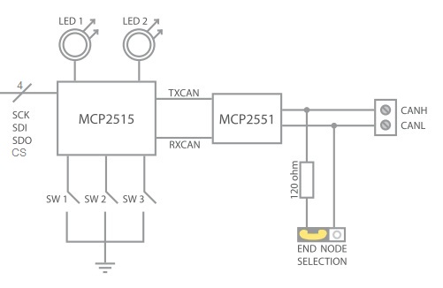
External CAN schematic

ExternalCAN.jpg


CAN Message Decoding

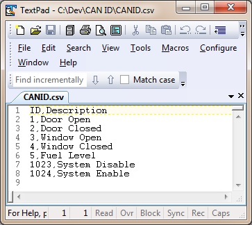
The CAN component works together with the injector component to allow you to decode a CAN message ID into a meaningful command.


Example File FC6 Icon.png CAN_Example1 When a key on the keypad is pressed the CAN components transmits a CAN packet.

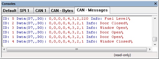
The CAN packet is decoded by the injector component to give us a meaningful log on the console window.


High Level CAN Data Console

CAN High.jpg


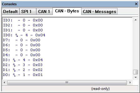
Low Level CAN Data Console

CAN Low.jpg


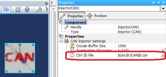
Reference from CAN Injector to ID decode file, $(srcdir) refers to the current project directory.

CAN File.jpg


Demo CAN ID file File:CANID.csv

CAN DataFile.jpg


CAN Masks and Filters

How to work out which messages will be trapped by a particular mask/filter combination

Note that all values for message id's, masks and filters are numbers between 0x000 and 0x7FF.


Example 1


Mask0 = 0x0FF

Filter0 = 0x100

Filter1 = 0x050


In binary, this looks like:


Mask0 = 000 1111 1111

Filter0 = 001 0000 0000

Filter1 = 000 0101 0000


For the mask, a "1" signifies "check this bit" and a "0" means "ignore this bit"


So, these filters will accept the following messages ("x" = don't care)


Filter0 = xxx 0000 0000

Filter1 = xxx 0101 0000


i.e.


Filter0 = 0x000, 0x100, 0x200, 0x300, 0x400, 0x500, 0x600, 0x700

Filter1 = 0x050, 0x150, 0x250, 0x350, 0x450, 0x550, 0x650, 0x750


Example 2


Mask1 = 0x350

Filter2 = 0x200

Filter3 = 0x123

Filter4 = 0x3FF


Rewriting in binary:


Mask1 = 111 0101 0000

Filter2 = 010 0000 0000

Filter3 = 001 0010 0011

Filter4 = 111 1111 1111


Here, the mask will only check 4 bits and ignore the other 6. Here's what the filters will accept:


Filter2 = 010 x0x0 xxxx

Filter3 = 001 x0x0 xxxx

Filter4 = 111 x1x1 xxxx


They will actually trap a lot of messages (64 each!):


Filter2 = 0x200, 0x201, 0x202, ... 0x220, 0x221, ... 0x280, 0x281, ... 0x2A0, 0x2A1, ... 0x2AF

Filter3 = 0x100, 0x101, 0x102, ... 0x120, 0x121, ... 0x180, 0x181, ... 0x1A0, 0x1A1, ... 0x1AF

Filter4 = 0x750, 0x751, 0x752, ... 0x770, 0x771, ... 0x7D0, 0x7D1, ... 0x7F0, 0x7F1, ... 0x7FF


This second example is not very practical. In general, it is more logical to set the mask so that each filter accepts a consecutive range of messages.


As you can see, the mask determines which bits of the filters are actually looked at. Setting the mask to 0x000 will effectively mean that the filter will accept any incoming message. Also, the value of the mask directly relates to how many messages each filter will trap - i.e. 2^(number of '0' bits in the mask).


A useful way to use the mask would be to ignore the least significant bits. Lets say that you wanted the filters to accept 16 messages each - setting the Mask0 to 0x7F0 would achieve this. Then, setting the filters to the following:


Filter0 = 0x100

Filter1 = 0x110


would mean that the following messages are accepted:


Filter0 = 0x100, 0x101, 0x102, 0x103, 0x104, ... 0x10D, 0x10E, 0x10F

Filter1 = 0x110, 0x111, 0x112, 0x113, 0x114, ... 0x11D, 0x11E, 0x11F


Of course, for simple CAN applications you may wish to only accept one or two messages. Setting the mask to 0x7FF in this instance would mean that only the message ID specified by each filter would be accepted, e.g.


Mask1 = 0x7FF

Filter2 = 0x100

Filter5 = 0x200


This would mean that only messages 0x100 and 0x200 would be accepted into buffer 1.

Downloadable macro reference

Fc9-comp-macro.png ReadSwitches
Returns switch input states from the external MCP2515 device. 0 = No Switch Pressed, 1 = Switch 1 Pressed, 2 = Switch 2 Pressed, 3 = Both Pressed (External CAN only)  
Fc9-u8-icon.png - BYTE Return


Fc9-comp-macro.png SetTxData
Assigns one of the outgoing transmit buffers with data ready to be sent. 
Fc9-u8-icon.png - BYTE Buffer
 
Fc9-u8-icon.png - BYTE Count
 
Fc9-u8-icon.png - BYTE d0
 
Fc9-u8-icon.png - BYTE d1
 
Fc9-u8-icon.png - BYTE d2
 
Fc9-u8-icon.png - BYTE d3
 
Fc9-u8-icon.png - BYTE d4
 
Fc9-u8-icon.png - BYTE d5
 
Fc9-u8-icon.png - BYTE d6
 
Fc9-u8-icon.png - BYTE d7
 
Fc9-void-icon.png - VOID Return


Fc9-comp-macro.png SetRxMask
Allows the receive ID mask to be configured on the fly allowing different ID ranges to be received. 
Fc9-u8-icon.png - BYTE Mask
Specifies which receive mask to modify. Range: 0-1 
Fc9-u32-icon.png - ULONG ID
The ID mask value you wish to use 
Fc9-void-icon.png - VOID Return


Fc9-comp-macro.png GetRxData
Returns last received message data byte at position Index. Buffer parameter is currently ignored 
Fc9-u8-icon.png - BYTE Buffer
 
Fc9-u8-icon.png - BYTE Index
 
Fc9-u8-icon.png - BYTE Return


Fc9-comp-macro.png GetRxIDHi
Gets the Hi byte Rx ID in register format. Standard ID only 0-2047. Compatible with v5 component and previous,  
Fc9-u8-icon.png - BYTE Buffer
Receive Buffer. Range 0-1 
Fc9-u8-icon.png - BYTE Return


Fc9-comp-macro.png SetTxIDSimple
Set the Tx CAN ID as a generic number. Standard IDs only 0-2047.  
Fc9-u8-icon.png - BYTE Buffer
Transmit buffer to load. Range: 0-2 
Fc9-u16-icon.png - UINT ID
The ID value you wish to use. Range: 0-2047 
Fc9-void-icon.png - VOID Return


Fc9-comp-macro.png SendBuffer
Transmits one of the transmit buffers which should have already been populated with an ID and data. 
Fc9-u8-icon.png - BYTE Buffer
Specifies which transmit buffer to send 
Fc9-void-icon.png - VOID Return


Fc9-comp-macro.png GetRxDataCount
Returns last received message data length. Buffer parameter is currently ignored 
Fc9-u8-icon.png - BYTE Buffer
 
Fc9-u8-icon.png - BYTE Return


Fc9-comp-macro.png SetRxFilterID
sets the Filter Standard mode only (for V5 compatibility only) 
Fc9-u8-icon.png - BYTE Filter
Specifies which filter to modify. Range: 0-5 
Fc9-u8-icon.png - BYTE Hi
ID bits 3-10 
Fc9-u8-icon.png - BYTE Lo
ID bits 0-2 stored in the upper 3 bits of the byte 
Fc9-void-icon.png - VOID Return


Fc9-comp-macro.png GetRxIDLo
Gets the Lo byte Rx ID in register format. Standard ID only 0-2047. Compatible with v5 component and previous,  
Fc9-u8-icon.png - BYTE Buffer
 
Fc9-u8-icon.png - BYTE Return


Fc9-comp-macro.png SetRxMaskID
set the Mask Standard ID mode only (for V5 compatibility)  
Fc9-u8-icon.png - BYTE Mask
Specifies which receive mask to modify. Range: 0-1 
Fc9-u8-icon.png - BYTE Hi
ID bits 3-10 
Fc9-u8-icon.png - BYTE Lo
ID bits 0-2 stored in the upper 3 bits of the byte 
Fc9-void-icon.png - VOID Return


Fc9-comp-macro.png SetRxFilter
Allows the receive ID filter to be configured on the fly allowing different ID ranges to be received. 
Fc9-u8-icon.png - BYTE Filter
Specifies which receive filter to modify. Range: 0-5 
Fc9-u32-icon.png - ULONG ID
The ID filter value you wish to use 
Fc9-void-icon.png - VOID Return


Fc9-comp-macro.png SetTxIdent
Set the Tx CAN ID as a generic number. Standard and extended IDs Standard 0-2047 Extended 2048-536870911  
Fc9-u8-icon.png - BYTE Buffer
Transmit buffer to load. Range: 0-2 
Fc9-u32-icon.png - ULONG ID
The ID or Extended ID value you wish to use. Range: 0-536870911 
Fc9-void-icon.png - VOID Return


Fc9-comp-macro.png CheckRx
Checks to see if any messages are available for 'Buffer' specified  
Fc9-u8-icon.png - BYTE Buffer
Send buffer: 0 to 1 
Fc9-u8-icon.png - BYTE Return


Fc9-comp-macro.png GetRxIDSimple
Gets the Rx ID as a Integer Standard ID only 0-2047. 
Fc9-u8-icon.png - BYTE Buffer
Receive Buffer. Range 0-1 
Fc9-u16-icon.png - UINT Return


Fc9-comp-macro.png SetTxID
Set the Tx CAN ID in register format. Standard ID only 0-2047. Compatible with v5 component and previous, 
Fc9-u8-icon.png - BYTE Buffer
Transmit buffer to load. Range: 0-2 
Fc9-u8-icon.png - BYTE Hi
ID bits 3-10 e.g. ((ID & 0x7F8) >> 3) 
Fc9-u8-icon.png - BYTE Lo
ID bits 0-2 stored in the upper 3 bits of the byte e.g. ((ID & 0x7) << 5) 
Fc9-void-icon.png - VOID Return


Fc9-comp-macro.png ShowLEDs
Set LED state (External CAN only)  
Fc9-u8-icon.png - BYTE led1
Controls LED 1. Range: 0-1 
Fc9-u8-icon.png - BYTE led2
Controls LED 2. Range: 0-1 
Fc9-void-icon.png - VOID Return


Fc9-comp-macro.png GetRxIdent
Gets the Rx ID as a Integer Standard and Extended IDs. 
Fc9-u8-icon.png - BYTE Buffer
 
Fc9-u32-icon.png - ULONG Return


Fc9-comp-macro.png Initialise
Must be called before any other CAN component macros to enable and initialise the CAN peripheral.  
Fc9-void-icon.png - VOID Return


Property reference

Fc9-prop-icon.png Properties
Fc9-type-16-icon.png Channel
Switches between Internal CAN peripheral and External CAN controller IC MCP2515. 
Fc9-type-16-icon.png Controller Osc
 
Fc9-type-16-icon.png Bus Rate
Data rate of the bus specified in thousand bits per second, Kbps. 
Fc9-type-16-icon.png Sync Jump Width
Defines how far a resyncronisation may move the sample point 
Fc9-type-16-icon.png Sample Point
Point in each bit period where the incoming data is sampled. 
Fc9-type-16-icon.png ID Type
Switches between using Standard, or Standard and Extended CAN 
Fc9-type-16-icon.png One Shot Mode
Disabled. Messages will reattempt transmission Enabled. Message will only attempt to transmit once 
Fc9-type-16-icon.png CHANNEL
SPI Channel selector 
Fc9-type-5-icon.png MOSI
SPI Data Out Pin SDO - Also Known as Master Out Slave In (MOSI) when used in Master mode. 
Fc9-type-5-icon.png MISO
SPI Data In Pin SDI - Also Known as Master In Slave Out (MISO) when used in Master mode. 
Fc9-type-5-icon.png CLK
SPI Clock Pin CLK - The Clock signal is driven by the SPI master. 
Fc9-type-5-icon.png SS
Chip Select / Slave Select Pin Master Mode: General purpose output pin used to select the remote SPI device. Slave Mode: Hardware chip select pin input used to select the SPI device.  
Fc9-type-16-icon.png Prescale
Prescale option selector 
Fc9-type-16-icon.png Sample Point
Data bit read sample point 
Fc9-type-16-icon.png Config Delay
 
Fc9-type-5-icon.png TX Pin
Internal CAN TX Pin 
Fc9-type-16-icon.png TX Remap
Internal CAN Tx Remap Pin 
Fc9-type-5-icon.png RX Pin
Internal CAN Rx Pin 
Fc9-type-16-icon.png RX Remap
Internal CAN Rx Remap Pin 
Fc9-type-14-icon.png Message ID
TX Buffer 0 Message Identifier 
Fc9-type-14-icon.png Length
TX Buffer 0 Number of data bytes 
Fc9-type-14-icon.png D0
TX Buffer 0 Data Byte 0 
Fc9-type-14-icon.png D1
TX Buffer 0 Data Byte 1 
Fc9-type-14-icon.png D2
TX Buffer 0 Data Byte 2 
Fc9-type-14-icon.png D3
TX Buffer 0 Data Byte 3 
Fc9-type-14-icon.png D4
TX Buffer 0 Data Byte 4 
Fc9-type-14-icon.png D5
TX Buffer 0 Data Byte 5 
Fc9-type-14-icon.png D6
TX Buffer 0 Data Byte 6 
Fc9-type-14-icon.png D7
TX Buffer 0 Data Byte 7 
Fc9-type-14-icon.png Message ID
TX Buffer 1 Message Identifier 
Fc9-type-14-icon.png Length
TX Buffer 1 Number of data bytes 
Fc9-type-14-icon.png D0
TX Buffer 1 Data Byte 0 
Fc9-type-14-icon.png D1
TX Buffer 1 Data Byte 1 
Fc9-type-14-icon.png D2
TX Buffer 1 Data Byte 2 
Fc9-type-14-icon.png D3
TX Buffer 1 Data Byte 3 
Fc9-type-14-icon.png D4
TX Buffer 1 Data Byte 4 
Fc9-type-14-icon.png D5
TX Buffer 1 Data Byte 5 
Fc9-type-14-icon.png D6
TX Buffer 1 Data Byte 6 
Fc9-type-14-icon.png D7
TX Buffer 1 Data Byte 7 
Fc9-type-14-icon.png Message ID
TX Buffer 2 Message Identifier 
Fc9-type-14-icon.png Length
TX Buffer 2 Number of data bytes 
Fc9-type-14-icon.png D0
TX Buffer 2 Data Byte 0 
Fc9-type-14-icon.png D1
TX Buffer 2 Data Byte 1 
Fc9-type-14-icon.png D2
TX Buffer 2 Data Byte 2 
Fc9-type-14-icon.png D3
TX Buffer 2 Data Byte 3 
Fc9-type-14-icon.png D4
TX Buffer 2 Data Byte 4 
Fc9-type-14-icon.png D5
TX Buffer 2 Data Byte 5 
Fc9-type-14-icon.png D6
TX Buffer 2 Data Byte 6 
Fc9-type-14-icon.png D7
TX Buffer 2 Data Byte 7 
Fc9-type-16-icon.png Settings
RX Buffer 0 Message Receive Mode 
Fc9-type-16-icon.png Settings
RX Buffer 1 Message Receive Mode 
Fc9-type-7-icon.png Scope Traces
Selects if the scope traces are automatically generated or not 
Fc9-type-7-icon.png Console Data
Selects if the console data is automatically generated or not 
Fc9-type-16-icon.png API
 
Fc9-conn-icon.png Connections
Fc9-conn-icon.png Simulations
Fc9-type-10-icon.png Label
Comms Flasher Identification Label 
Fc9-type-7-icon.png Simulate SPI Comms