Difference between revisions of "Component: HBRIDGE (CAL) (Misc)"
From Flowcode Help
Jump to navigationJump to search (Created page with "{| style="width:50%" |- | width="20%" style="color:gray;" | Author | Matrix TSL |- | width="20%" style="color:gray;" | Version | 2.1 |- | width="20%" style="color:gray...") |
|||
| Line 15: | Line 15: | ||
CAL = Code Abstraction Layer - Allows one code base to run on a wide range of chips. A low level implementation giving direct access to the H-Bridge peripheral. Currently only supports compatible 8-bit PIC devices. | CAL = Code Abstraction Layer - Allows one code base to run on a wide range of chips. A low level implementation giving direct access to the H-Bridge peripheral. Currently only supports compatible 8-bit PIC devices. | ||
| − | ==Component | + | ==Component Source Code== |
| − | + | Please click here for the component source code: [https://www.flowcode.co.uk/wikicopy/componentsource/FC_Comp_Source_HBRIDGE.fcfx FC_Comp_Source_HBRIDGE.fcfx] | |
==Detailed description== | ==Detailed description== | ||
| + | |||
| + | |||
| Line 45: | Line 47: | ||
==Examples== | ==Examples== | ||
| + | |||
| + | |||
| Line 193: | Line 197: | ||
| width="10%" align="center" style="background-color:#D8C9D8;" | [[File:Fc9-prop-icon.png]] | | width="10%" align="center" style="background-color:#D8C9D8;" | [[File:Fc9-prop-icon.png]] | ||
| width="90%" style="background-color:#D8C9D8; color:#4B008D;" | '''Properties''' | | width="90%" style="background-color:#D8C9D8; color:#4B008D;" | '''Properties''' | ||
| + | |- | ||
| + | |- | ||
| + | | width="10%" align="center" style="background-color:#EAE1EA;" | [[File:Fc9-conn-icon.png]] | ||
| + | | width="90%" style="background-color:#EAE1EA; color:#4B008D;" | Settings | ||
|- | |- | ||
|- | |- | ||
| Line 229: | Line 237: | ||
|- | |- | ||
| colspan="2" | PWM Period Register value | | colspan="2" | PWM Period Register value | ||
| + | |- | ||
| + | | width="10%" align="center" style="background-color:#EAE1EA;" | [[File:Fc9-conn-icon.png]] | ||
| + | | width="90%" style="background-color:#EAE1EA; color:#4B008D;" | Dead Band | ||
| + | |- | ||
|- | |- | ||
| width="10%" align="center" | [[File:Fc9-type-21-icon.png]] | | width="10%" align="center" | [[File:Fc9-type-21-icon.png]] | ||
| Line 250: | Line 262: | ||
| colspan="2" | Number of cycles to wait after a rising edge and before a falling edge. | | colspan="2" | Number of cycles to wait after a rising edge and before a falling edge. | ||
|- | |- | ||
| − | + | | width="10%" align="center" style="background-color:#EAE1EA;" | [[File:Fc9-conn-icon.png]] | |
| − | + | | width="90%" style="background-color:#EAE1EA; color:#4B008D;" | Connections | |
| − | |||
| − | |||
| − | |||
| − | |||
| − | |||
| − | |||
| − | |||
| − | |||
| − | |||
| − | |||
| − | |||
| − | |||
| − | |||
| − | |||
| − | |||
| − | |||
| − | |||
| − | |||
| − | | width="10%" align="center" style="background-color:# | ||
| − | | width="90%" style="background-color:# | ||
|- | |- | ||
|- | |- | ||
| Line 314: | Line 306: | ||
| colspan="2" | Remap Pin D - Specifies the pin used for the D output. Only available on devices supporting remappable hardware pins. | | colspan="2" | Remap Pin D - Specifies the pin used for the D output. Only available on devices supporting remappable hardware pins. | ||
|- | |- | ||
| − | | width="10%" align="center" style="background-color:# | + | | width="10%" align="center" style="background-color:#EAE1EA;" | [[File:Fc9-conn-icon.png]] |
| − | | width="90%" style="background-color:# | + | | width="90%" style="background-color:#EAE1EA; color:#4B008D;" | Calculations |
| + | |- | ||
| + | |- | ||
| + | | width="10%" align="center" | [[File:Fc9-type-14-icon.png]] | ||
| + | | width="90%" | Clock Speed | ||
| + | |- | ||
| + | | colspan="2" | Target Microcontroller Clock Speed. | ||
| + | |- | ||
| + | | width="10%" align="center" | [[File:Fc9-type-15-icon.png]] | ||
| + | | width="90%" | Period (uS) | ||
| + | |- | ||
| + | | colspan="2" | Calculated length of PWM period in micro seconds. | ||
| + | |- | ||
| + | | width="10%" align="center" | [[File:Fc9-type-15-icon.png]] | ||
| + | | width="90%" | Frequency (KHz) | ||
| + | |- | ||
| + | | colspan="2" | Calculated PWM output frequency in KHz. | ||
| + | |- | ||
| + | | width="10%" align="center" | [[File:Fc9-type-15-icon.png]] | ||
| + | | width="90%" | Frequency (Hz) | ||
|- | |- | ||
| + | | colspan="2" | Calculated PWM output frequency in Hz. | ||
|} | |} | ||
Revision as of 17:47, 9 November 2022
| Author | Matrix TSL |
| Version | 2.1 |
| Category | Misc |
Contents
HBRIDGE component
CAL = Code Abstraction Layer - Allows one code base to run on a wide range of chips. A low level implementation giving direct access to the H-Bridge peripheral. Currently only supports compatible 8-bit PIC devices.
Component Source Code
Please click here for the component source code: FC_Comp_Source_HBRIDGE.fcfx
Detailed description
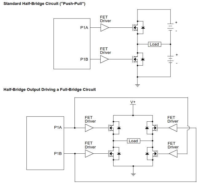
Half Bridge Application
A Half Bridge type output has two output signals A and B.
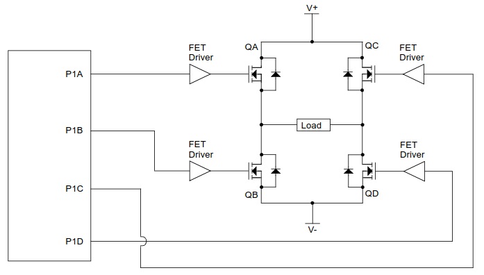
Full Bridge Application
Full Bridge type output has four output signals A, B, C and D.
Examples
A simple proof of concept example to drive a full bridge output with varying speed and direction.
Downloadable macro reference
| GetValue | |
| Returns Named property Value | |
| Name | |
| Return | |
| Disable | |
| Disable this PWM Channel | |
| Return | |
| Enable | |
| Enable this PWM Channel | |
| Return | |
| SetSpeed | |
| Sets the motor speed by varying the PWM duty. | |
| duty | |
| Duty value 0 - 1023 | |
| Return | |
| SetValue | |
| Sets the Value of the property PERIOD, PRESCALE or CHANNEL (if CHANNEL also updates the PORT from FCD) | |
| Name | |
| Value | |
| Return | |
| SetDirection | |
| Set the motor direction. | |
| direction | |
| 0 = Forwards, 1 = Reverse | |
| Return | |
| GetList | |
| Returns CHANNEL or PRESCALE list from the FCD and updates the internal property | |
| Name | |
| Return | |

