Difference between revisions of "Component: ADC (AD7680) (Analog Input)"
From Flowcode Help
Jump to navigationJump to search| Line 94: | Line 94: | ||
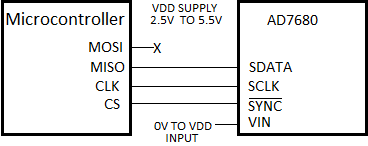
==Circuit Diagram== | ==Circuit Diagram== | ||
[[File:AD7680 Circuit Diagram.png]] | [[File:AD7680 Circuit Diagram.png]] | ||
| + | |||
| + | |||
| Line 101: | Line 103: | ||
==Macro reference== | ==Macro reference== | ||
| + | ===SampleADC=== | ||
{| class="wikitable" style="width:60%; background-color:#FFFFFF;" | {| class="wikitable" style="width:60%; background-color:#FFFFFF;" | ||
|- | |- | ||
| Line 114: | Line 117: | ||
| + | ===Initialise=== | ||
{| class="wikitable" style="width:60%; background-color:#FFFFFF;" | {| class="wikitable" style="width:60%; background-color:#FFFFFF;" | ||
|- | |- | ||
Revision as of 11:49, 3 February 2023
| Author | Matrix TSL |
| Version | 1.0 |
| Category | Analog Input |
Contents
ADC (AD7680) component
16-bit external ADC connected to the microcontroller using SPI.
Component Source Code
Please click here to download the component source project: FC_Comp_Source_ExternalADC_AD7680.fcfx
Please click here to view the component source code (Beta): FC_Comp_Source_ExternalADC_AD7680.fcfx
Detailed description
Overview
The AD7680 is a 2.5V to 5.5V SPI compatible, successive approximation analogue to digital converter (ADC).
The reference for the AD7680 is taken internally from VDD
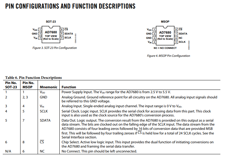
Pin reference from the datasheet:
Examples
This example reads the voltage on the AD7680 Vin and converts the ADC results into a voltage. For the result to be correct, you must change the Voltage variable to match the supply voltage.
Circuit Diagram
Macro reference
SampleADC
| SampleADC | |
| Reads the ADC and returns the reading as an unsigned 16-bit value. Range: 0-65535 / 0=0V / 65535=VCC | |
| Return | |
Initialise
| Initialise | |
| Initialise the SPI bus ready for communications, | |
| Return | |

