|
|
| (11 intermediate revisions by 3 users not shown) |
| Line 22: |
Line 22: |
|
| |
|
| ==Detailed description== | | ==Detailed description== |
| | |
| | |
|
| |
|
|
| |
|
| Line 59: |
Line 61: |
|
| |
|
| ==Examples== | | ==Examples== |
|
| |
|
| |
|
| |
|
| |
|
| |
|
| |
|
| |
|
| |
|
| |
|
| |
|
| |
|
| |
|
| |
|
| |
|
| |
|
| |
|
| |
|
| |
|
| |
|
| |
|
| |
|
| |
|
| |
|
| |
|
| |
|
| This example reads the voltage on the AD7680 Vin and converts the ADC results into a voltage. | | This example reads the voltage on the AD7680 Vin and converts the ADC results into a voltage. |
| Line 88: |
Line 66: |
|
| |
|
| {{Fcfile|AD7680 Demo.fcfx|AD7680 Demo}} | | {{Fcfile|AD7680 Demo.fcfx|AD7680 Demo}} |
| | |
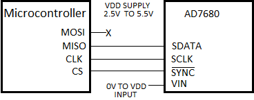
| ==Circuit Diagram== | | ==Circuit Diagram== |
| [[File:AD7680 Circuit Diagram.png]] | | [[File:AD7680 Circuit Diagram.png]] |
| Line 93: |
Line 72: |
|
| |
|
|
| |
|
| ==Macro reference==
| |
|
| |
|
| {| class="wikitable" style="width:60%; background-color:#FFFFFF;"
| |
| |-
| |
| | width="10%" align="center" style="background-color:#D8C9D8;" align="center" | [[File:Fc9-comp-macro.png]]
| |
| | width="90%" style="background-color:#D8C9D8; color:#4B008D;" | '''SampleADC'''
| |
| |-
| |
| | colspan="2" | Reads the ADC and returns the reading as an unsigned 16-bit value. Range: 0-65535 / 0=0V / 65535=VCC
| |
| |-
| |
| |-
| |
| | width="10%" align="center" style="border-top: 2px solid #000;" | [[File:Fc9-u16-icon.png]] - UINT
| |
| | width="90%" style="border-top: 2px solid #000;" | ''Return''
| |
| |}
| |
|
| |
|
|
| |
|
| {| class="wikitable" style="width:60%; background-color:#FFFFFF;"
| |
| |-
| |
| | width="10%" align="center" style="background-color:#D8C9D8;" align="center" | [[File:Fc9-comp-macro.png]]
| |
| | width="90%" style="background-color:#D8C9D8; color:#4B008D;" | '''Initialise'''
| |
| |-
| |
| | colspan="2" | Initialise the SPI bus ready for communications,
| |
| |-
| |
| |-
| |
| | width="10%" align="center" style="border-top: 2px solid #000;" | [[File:Fc9-void-icon.png]] - VOID
| |
| | width="90%" style="border-top: 2px solid #000;" | ''Return''
| |
| |}
| |
|
| |
|
| |
|
| |
|
| |
| ==Property reference==
| |
|
| |
| {| class="wikitable" style="width:60%; background-color:#FFFFFF;"
| |
| |-
| |
| | width="10%" align="center" style="background-color:#D8C9D8;" | [[File:Fc9-prop-icon.png]]
| |
| | width="90%" style="background-color:#D8C9D8; color:#4B008D;" | '''Properties'''
| |
| |-
| |
| |-
| |
| | width="10%" align="center" style="background-color:#EAE1EA;" | [[File:Fc9-conn-icon.png]]
| |
| | width="90%" style="background-color:#EAE1EA; color:#4B008D;" | SPI Properties
| |
| |-
| |
| |-
| |
| | width="10%" align="center" | [[File:Fc9-type-16-icon.png]]
| |
| | width="90%" | Channel
| |
| |-
| |
| | colspan="2" | SPI Channel selector
| |
| |-
| |
| | width="10%" align="center" | [[File:Fc9-type-16-icon.png]]
| |
| | width="90%" | Prescale
| |
| |-
| |
| | colspan="2" | Prescale option selector
| |
| |-
| |
| | width="10%" align="center" | [[File:Fc9-type-5-icon.png]]
| |
| | width="90%" | MOSI
| |
| |-
| |
| | colspan="2" | SPI Data Out Pin SDO - Also Known as Master Out Slave In (MOSI) when used in Master mode.
| |
| |-
| |
| | width="10%" align="center" | [[File:Fc9-type-5-icon.png]]
| |
| | width="90%" | MISO
| |
| |-
| |
| | colspan="2" | SPI Data In Pin SDI - Also Known as Master In Slave Out (MISO) when used in Master mode.
| |
| |-
| |
| | width="10%" align="center" | [[File:Fc9-type-5-icon.png]]
| |
| | width="90%" | CLK
| |
| |-
| |
| | colspan="2" | SPI Clock Pin CLK - The Clock signal is driven by the SPI master.
| |
| |-
| |
| | width="10%" align="center" | [[File:Fc9-type-5-icon.png]]
| |
| | width="90%" | CS / SS
| |
| |-
| |
| | colspan="2" | Chip Select / Slave Select Pin Master Mode: General purpose output pin used to select the remote SPI device. Slave Mode: Hardware chip select pin input used to select the SPI device.
| |
| |-
| |
| | width="10%" align="center" style="background-color:#EAE1EA;" | [[File:Fc9-conn-icon.png]]
| |
| | width="90%" style="background-color:#EAE1EA; color:#4B008D;" | Simulation
| |
| |-
| |
| |-
| |
| | width="10%" align="center" | [[File:Fc9-type-7-icon.png]]
| |
| | width="90%" | Data Recorder Trace
| |
| |-
| |
| | colspan="2" |
| |
| |-
| |
| | width="10%" align="center" | [[File:Fc9-type-7-icon.png]]
| |
| | width="90%" | Simulate Comms
| |
| |-
| |
| | colspan="2" |
| |
| |}==Macro reference==
| |
|
| |
|
| {| class="wikitable" style="width:60%; background-color:#FFFFFF;"
| |
| |-
| |
| | width="10%" align="center" style="background-color:#D8C9D8;" align="center" | [[File:Fc9-comp-macro.png]]
| |
| | width="90%" style="background-color:#D8C9D8; color:#4B008D;" | '''SampleADC'''
| |
| |-
| |
| | colspan="2" | Reads the ADC and returns the reading as an unsigned 16-bit value. Range: 0-65535 / 0=0V / 65535=VCC
| |
| |-
| |
| |-
| |
| | width="10%" align="center" style="border-top: 2px solid #000;" | [[File:Fc9-u16-icon.png]] - UINT
| |
| | width="90%" style="border-top: 2px solid #000;" | ''Return''
| |
| |}
| |
|
| |
|
|
| |
|
| {| class="wikitable" style="width:60%; background-color:#FFFFFF;"
| |
| |-
| |
| | width="10%" align="center" style="background-color:#D8C9D8;" align="center" | [[File:Fc9-comp-macro.png]]
| |
| | width="90%" style="background-color:#D8C9D8; color:#4B008D;" | '''Initialise'''
| |
| |-
| |
| | colspan="2" | Initialise the SPI bus ready for communications,
| |
| |-
| |
| |-
| |
| | width="10%" align="center" style="border-top: 2px solid #000;" | [[File:Fc9-void-icon.png]] - VOID
| |
| | width="90%" style="border-top: 2px solid #000;" | ''Return''
| |
| |}
| |
|
| |
|
|
| |
|
|
| |
|
|
| |
|
| ==Property reference==
| | ==Macro reference== |
| | |
| {| class="wikitable" style="width:60%; background-color:#FFFFFF;"
| |
| |-
| |
| | width="10%" align="center" style="background-color:#D8C9D8;" | [[File:Fc9-prop-icon.png]]
| |
| | width="90%" style="background-color:#D8C9D8; color:#4B008D;" | '''Properties'''
| |
| |-
| |
| |-
| |
| | width="10%" align="center" style="background-color:#EAE1EA;" | [[File:Fc9-conn-icon.png]]
| |
| | width="90%" style="background-color:#EAE1EA; color:#4B008D;" | SPI Properties
| |
| |-
| |
| |-
| |
| | width="10%" align="center" | [[File:Fc9-type-16-icon.png]]
| |
| | width="90%" | Channel
| |
| |-
| |
| | colspan="2" | SPI Channel selector
| |
| |-
| |
| | width="10%" align="center" | [[File:Fc9-type-16-icon.png]]
| |
| | width="90%" | Prescale
| |
| |-
| |
| | colspan="2" | Prescale option selector
| |
| |-
| |
| | width="10%" align="center" | [[File:Fc9-type-5-icon.png]]
| |
| | width="90%" | MOSI
| |
| |-
| |
| | colspan="2" | SPI Data Out Pin SDO - Also Known as Master Out Slave In (MOSI) when used in Master mode.
| |
| |-
| |
| | width="10%" align="center" | [[File:Fc9-type-5-icon.png]]
| |
| | width="90%" | MISO
| |
| |-
| |
| | colspan="2" | SPI Data In Pin SDI - Also Known as Master In Slave Out (MISO) when used in Master mode.
| |
| |-
| |
| | width="10%" align="center" | [[File:Fc9-type-5-icon.png]]
| |
| | width="90%" | CLK
| |
| |-
| |
| | colspan="2" | SPI Clock Pin CLK - The Clock signal is driven by the SPI master.
| |
| |-
| |
| | width="10%" align="center" | [[File:Fc9-type-5-icon.png]]
| |
| | width="90%" | CS / SS
| |
| |-
| |
| | colspan="2" | Chip Select / Slave Select Pin Master Mode: General purpose output pin used to select the remote SPI device. Slave Mode: Hardware chip select pin input used to select the SPI device.
| |
| |-
| |
| | width="10%" align="center" style="background-color:#EAE1EA;" | [[File:Fc9-conn-icon.png]]
| |
| | width="90%" style="background-color:#EAE1EA; color:#4B008D;" | Simulation
| |
| |-
| |
| |-
| |
| | width="10%" align="center" | [[File:Fc9-type-7-icon.png]]
| |
| | width="90%" | Data Recorder Trace
| |
| |-
| |
| | colspan="2" |
| |
| |-
| |
| | width="10%" align="center" | [[File:Fc9-type-7-icon.png]]
| |
| | width="90%" | Simulate Comms
| |
| |-
| |
| | colspan="2" |
| |
| |}==Macro reference==
| |
|
| |
|
| {| class="wikitable" style="width:60%; background-color:#FFFFFF;" | | ===Initialise=== |
| | {| class="mtx-class-macrotable wikitable" |
| |- | | |- |
| | width="10%" align="center" style="background-color:#D8C9D8;" align="center" | [[File:Fc9-comp-macro.png]] | | | width="10%" align="center" class="mtx-class-macrohead" | [[File:Fc9-comp-macro.png]] |
| | width="90%" style="background-color:#D8C9D8; color:#4B008D;" | '''SampleADC''' | | | width="90%" class="mtx-class-macrohead" | '''Initialise''' |
| |-
| |
| | colspan="2" | Reads the ADC and returns the reading as an unsigned 16-bit value. Range: 0-65535 / 0=0V / 65535=VCC
| |
| |-
| |
| |-
| |
| | width="10%" align="center" style="border-top: 2px solid #000;" | [[File:Fc9-u16-icon.png]] - UINT
| |
| | width="90%" style="border-top: 2px solid #000;" | ''Return''
| |
| |}
| |
| | |
| | |
| {| class="wikitable" style="width:60%; background-color:#FFFFFF;"
| |
| |-
| |
| | width="10%" align="center" style="background-color:#D8C9D8;" align="center" | [[File:Fc9-comp-macro.png]]
| |
| | width="90%" style="background-color:#D8C9D8; color:#4B008D;" | '''Initialise'''
| |
| |- | | |- |
| | colspan="2" | Initialise the SPI bus ready for communications, | | | colspan="2" | Initialise the SPI bus ready for communications, |
| Line 291: |
Line 98: |
|
| |
|
|
| |
|
| | | ===SampleADC=== |
| | | {| class="mtx-class-macrotable wikitable" |
| ==Property reference== | |
| | |
| {| class="wikitable" style="width:60%; background-color:#FFFFFF;" | |
| |-
| |
| | width="10%" align="center" style="background-color:#D8C9D8;" | [[File:Fc9-prop-icon.png]]
| |
| | width="90%" style="background-color:#D8C9D8; color:#4B008D;" | '''Properties'''
| |
| |-
| |
| |-
| |
| | width="10%" align="center" style="background-color:#EAE1EA;" | [[File:Fc9-conn-icon.png]]
| |
| | width="90%" style="background-color:#EAE1EA; color:#4B008D;" | SPI Properties
| |
| |-
| |
| |-
| |
| | width="10%" align="center" | [[File:Fc9-type-16-icon.png]]
| |
| | width="90%" | Channel
| |
| |-
| |
| | colspan="2" | SPI Channel selector
| |
| |-
| |
| | width="10%" align="center" | [[File:Fc9-type-16-icon.png]]
| |
| | width="90%" | Prescale
| |
| |-
| |
| | colspan="2" | Prescale option selector
| |
| |-
| |
| | width="10%" align="center" | [[File:Fc9-type-5-icon.png]]
| |
| | width="90%" | MOSI
| |
| |-
| |
| | colspan="2" | SPI Data Out Pin SDO - Also Known as Master Out Slave In (MOSI) when used in Master mode.
| |
| |-
| |
| | width="10%" align="center" | [[File:Fc9-type-5-icon.png]]
| |
| | width="90%" | MISO
| |
| |-
| |
| | colspan="2" | SPI Data In Pin SDI - Also Known as Master In Slave Out (MISO) when used in Master mode.
| |
| |-
| |
| | width="10%" align="center" | [[File:Fc9-type-5-icon.png]]
| |
| | width="90%" | CLK
| |
| |-
| |
| | colspan="2" | SPI Clock Pin CLK - The Clock signal is driven by the SPI master.
| |
| |-
| |
| | width="10%" align="center" | [[File:Fc9-type-5-icon.png]]
| |
| | width="90%" | CS / SS
| |
| |-
| |
| | colspan="2" | Chip Select / Slave Select Pin Master Mode: General purpose output pin used to select the remote SPI device. Slave Mode: Hardware chip select pin input used to select the SPI device.
| |
| |-
| |
| | width="10%" align="center" style="background-color:#EAE1EA;" | [[File:Fc9-conn-icon.png]]
| |
| | width="90%" style="background-color:#EAE1EA; color:#4B008D;" | Simulation
| |
| |-
| |
| |-
| |
| | width="10%" align="center" | [[File:Fc9-type-7-icon.png]]
| |
| | width="90%" | Data Recorder Trace
| |
| |-
| |
| | colspan="2" |
| |
| |-
| |
| | width="10%" align="center" | [[File:Fc9-type-7-icon.png]]
| |
| | width="90%" | Simulate Comms
| |
| |-
| |
| | colspan="2" |
| |
| |}==Macro reference==
| |
| | |
| {| class="wikitable" style="width:60%; background-color:#FFFFFF;"
| |
| |- | | |- |
| | width="10%" align="center" style="background-color:#D8C9D8;" align="center" | [[File:Fc9-comp-macro.png]] | | | width="10%" align="center" class="mtx-class-macrohead" | [[File:Fc9-comp-macro.png]] |
| | width="90%" style="background-color:#D8C9D8; color:#4B008D;" | '''SampleADC''' | | | width="90%" class="mtx-class-macrohead" | '''SampleADC''' |
| |- | | |- |
| | colspan="2" | Reads the ADC and returns the reading as an unsigned 16-bit value. Range: 0-65535 / 0=0V / 65535=VCC | | | colspan="2" | Reads the ADC and returns the reading as an unsigned 16-bit value. Range: 0-65535 / 0=0V / 65535=VCC |
| Line 361: |
Line 110: |
| | width="90%" style="border-top: 2px solid #000;" | ''Return'' | | | width="90%" style="border-top: 2px solid #000;" | ''Return'' |
| |} | | |} |
|
| |
|
| |
| {| class="wikitable" style="width:60%; background-color:#FFFFFF;"
| |
| |-
| |
| | width="10%" align="center" style="background-color:#D8C9D8;" align="center" | [[File:Fc9-comp-macro.png]]
| |
| | width="90%" style="background-color:#D8C9D8; color:#4B008D;" | '''Initialise'''
| |
| |-
| |
| | colspan="2" | Initialise the SPI bus ready for communications,
| |
| |-
| |
| |-
| |
| | width="10%" align="center" style="border-top: 2px solid #000;" | [[File:Fc9-void-icon.png]] - VOID
| |
| | width="90%" style="border-top: 2px solid #000;" | ''Return''
| |
| |}
| |
|
| |
|
| |
|
| |
|
|
| |
|
| ==Property reference== | | ==Property reference== |
|
| |
|
| {| class="wikitable" style="width:60%; background-color:#FFFFFF;" | | {| class="mtx-class-macrotable wikitable" |
| |- | | |- |
| | width="10%" align="center" style="background-color:#D8C9D8;" | [[File:Fc9-prop-icon.png]] | | | width="10%" align="center" class="mtx-class-macrohead" | [[File:Fc9-prop-icon.png]] |
| | width="90%" style="background-color:#D8C9D8; color:#4B008D;" | '''Properties''' | | | width="90%" class="mtx-class-macrohead" | '''Properties''' |
| |- | | |- |
| |- | | |- |
| | width="10%" align="center" style="background-color:#EAE1EA;" | [[File:Fc9-conn-icon.png]] | | | width="10%" align="center" class="mtx-class-propfolder" | [[File:Fc9-conn-icon.png]] |
| | width="90%" style="background-color:#EAE1EA; color:#4B008D;" | SPI Properties | | | width="90%" class="mtx-class-propfolder" | SPI Properties |
| |- | | |- |
| |- | | |- |
| Line 420: |
Line 154: |
| | colspan="2" | Chip Select / Slave Select Pin Master Mode: General purpose output pin used to select the remote SPI device. Slave Mode: Hardware chip select pin input used to select the SPI device. | | | colspan="2" | Chip Select / Slave Select Pin Master Mode: General purpose output pin used to select the remote SPI device. Slave Mode: Hardware chip select pin input used to select the SPI device. |
| |- | | |- |
| | width="10%" align="center" style="background-color:#EAE1EA;" | [[File:Fc9-conn-icon.png]] | | | width="10%" align="center" class="mtx-class-propfolder" | [[File:Fc9-conn-icon.png]] |
| | width="90%" style="background-color:#EAE1EA; color:#4B008D;" | Simulation | | | width="90%" class="mtx-class-propfolder" | Simulation |
| |- | | |- |
| |- | | |- |
| Author
|
Matrix TSL
|
| Version
|
1.0
|
| Category
|
Analog Input
|
ADC (AD7680) component
16-bit external ADC connected to the microcontroller using SPI.
Component Source Code
Please click here to download the component source project: FC_Comp_Source_ExternalADC_AD7680.fcfx
Please click here to view the component source code (Beta): FC_Comp_Source_ExternalADC_AD7680.fcfx
Detailed description
Overview
The AD7680 is a 2.5V to 5.5V SPI compatible, successive
approximation analogue to digital converter (ADC).
The reference for the AD7680 is taken internally from VDD
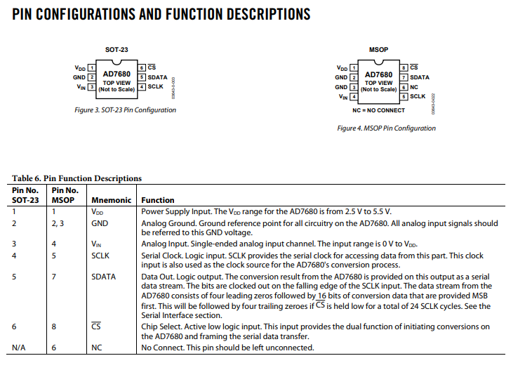
Pin reference from the datasheet:
Examples
This example reads the voltage on the AD7680 Vin and converts the ADC results into a voltage.
For the result to be correct, you must change the Voltage variable to match the supply voltage.
 AD7680 Demo
Circuit Diagram
Macro reference
Initialise

|
Initialise
|
| Initialise the SPI bus ready for communications,
|
 - VOID - VOID
|
Return
|
SampleADC
|
|
SampleADC
|
| Reads the ADC and returns the reading as an unsigned 16-bit value. Range: 0-65535 / 0=0V / 65535=VCC
|
 - UINT - UINT
|
Return
|
Property reference

|
Properties
|

|
SPI Properties
|

|
Channel
|
| SPI Channel selector
|
|
|
Prescale
|
| Prescale option selector
|

|
MOSI
|
| SPI Data Out Pin SDO - Also Known as Master Out Slave In (MOSI) when used in Master mode.
|
|
|
MISO
|
| SPI Data In Pin SDI - Also Known as Master In Slave Out (MISO) when used in Master mode.
|
|
|
CLK
|
| SPI Clock Pin CLK - The Clock signal is driven by the SPI master.
|
|
|
CS / SS
|
| Chip Select / Slave Select Pin Master Mode: General purpose output pin used to select the remote SPI device. Slave Mode: Hardware chip select pin input used to select the SPI device.
|
|
|
Simulation
|

|
Data Recorder Trace
|
|
|
|
|
Simulate Comms
|
|
|


 - VOID
 - UINT


